PX262 - K6 - energy gaps
- free electrons have the wave functions of the form:
, where - the energies are given by:so
-
linear combinations:
and -
these correspond to the same energy,
-
a 1D lattice will have the separations of
, and its reciprocal lattice, -
in the k-space, the first BZ:
-
looking at the free electron wavefunctions' intensities with
(values at the edges of the BZ): and
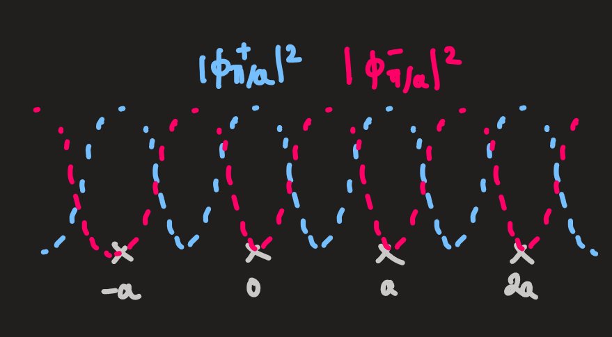
-
when potentials are placed on each of the lattice points, the energy degeneracy is broken, since
is distributed more closely to the potentials than the solution -
energy gaps at
are produced at the BZ boundaries -
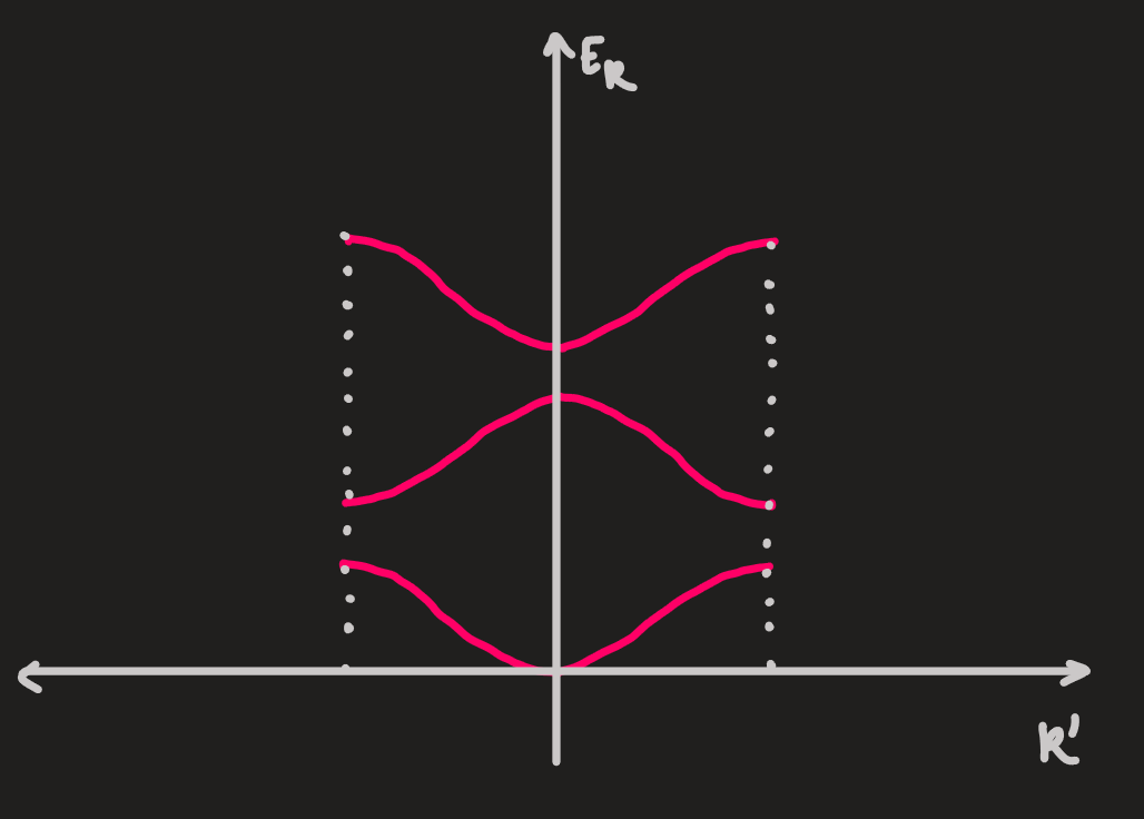
if the free electron model (1D) is perturbed by a weak crystalline potential, the electronic states change
-
this can be plotted in the first BZ, with
ie. folding back, or
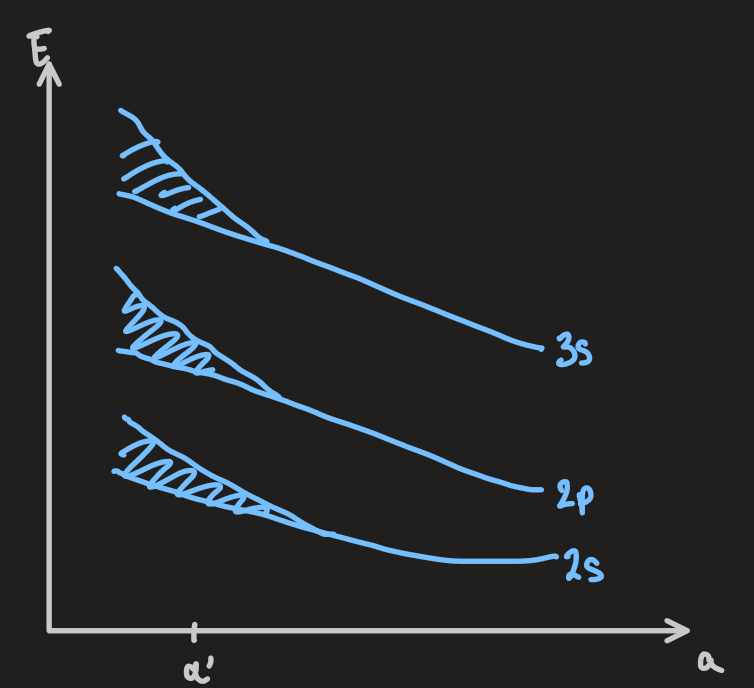
- a complementary insight can be obtained by starting with a model of a large number,
, of identical atoms, which are well separated. eg: Li: - each atom potential has a set of electronic energy levels for the valence electrons, eg:
- the energy level diagram for the whole system is set by that of a single atom, but the pauli exclusion principle for the entire system permits each state to be occupied by up to
(2 for spin) electrons
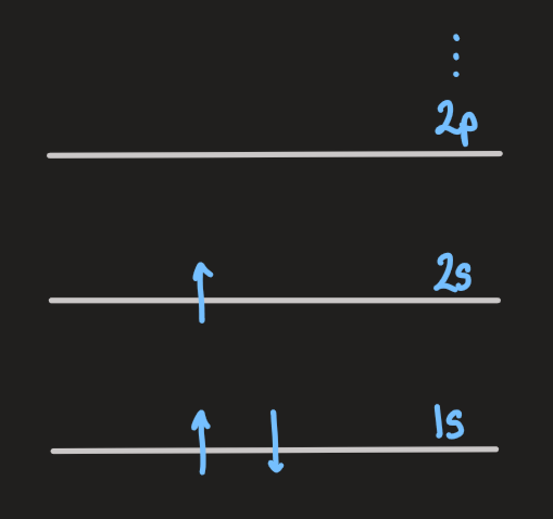
- if the atoms are pushed closer together, the wavefunctions of the electrons distort and extend over more atoms
- the outermost valence electronic states accommodate
in a band of tightly spaced levels
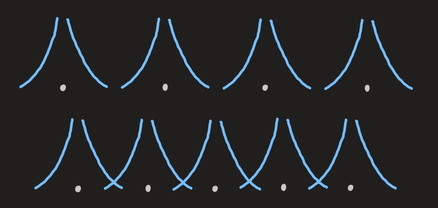
- the schematic for valence electrons of Li:
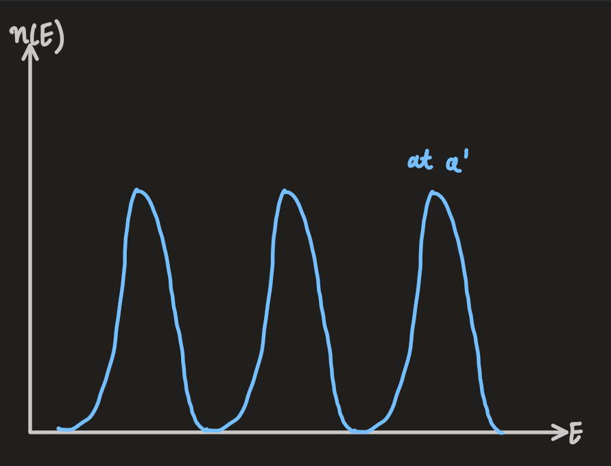
- the two figures above show how, in some materials, the DOS develops a gap at the fermi energy
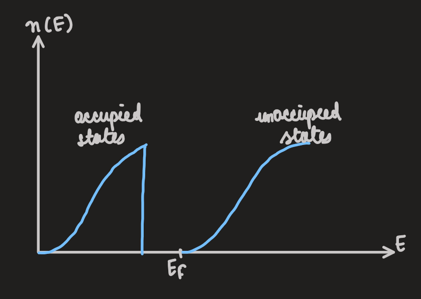
-
such a material is insulating
-
there are no states near
, no low-lying excitations and no conduction -
the specific heat has no electronic contribution for
-
the material is also transparent to light, with
and only photons with will be blocked -
a material is termed as an insulator if
eV, and for eV, the material is a semiconductor